
Minibadge Display Devboard
A small PCB that allows you to create your own Minibadge displays!

Introduction
What is it?
This board provides everything your custom Minibadge display will need, including LiPo battery charging/use and USB-C power. It can be attached board-to-board with your own PCB designs, or it can be wired up using push-in WAGO wire terminals to your existing displays.
Why did you make it?
I wanted to lower the barrier of entry for people creating their own custom minibadge displays - allowing designers to focus on the physical shapes, graphics, and layouts of custom displays. There are a lot of things to take into consideration and design for when making a Minibadge display.
- You must factor in power management
- Each minibadge should be allocated ~100mA. When you have tens to hundreds of minibadges, that's a lot of amps.
- Powerpath management becomes critical. You must have beefy regulators and often multiple power paths so a short or brownout does not take out the whole board.
- You must generate a clock signal for blinky LEDs
- Because this clock signal is push-pull, you must also amplify it using some sort of driver, as there can be a lot of inrush current.
- You must provide a 5v/batt+ rail (for regulators and minibadges)
- This means designing around USB and (optionally) a batteries.
- If you include batteries, you must have a BMS on board to charge the battery.
For many people getting started in the world of minibadges, that is a tall order to design around many disciplines they are unfamiliar with.
Goals
What did you want to achieve?
- A standalone PCB that gives your custom minibadge display
- battery or USB-C power
- 3.3v
- CLK
- GND
- VBATT/5V.
- Can support LiPo batteries, charging and discharging them, as well as temperature monitoring.
- Castellated edge-mount pads to facilitate board to board mounting.
- WAGO SMD push-in terminal blocks for custom wiring and non-permanent setups.
- Ensure battery can be charged while power switch is set to OFF
What are the limitations you ran into?
- USB-C without PD can carry at most 5V@3A (15W), but is more commonly limited to 5V@1.5A (7.5W)
- This means that, depending on how much current your minibadge draws, you can only power 30-50 minibadges.
- The maximum current that can charge the battery is 800mA, which is a limit of the BMS chip.
- Castellated pads are more expensive than I thought they would be. It's a $50+ setup fee regardless of order quantity.
- The regulator can only put out about 3A of 3.3V power.
Design Process
What references and tools did you use?
Components and their datasheets
- Voltage regulator - TLV62585RWT - https://www.ti.com/lit/ds/symlink/tlv62585.pdf
- Battery management system - BQ21040 - https://www.ti.com/lit/ds/symlink/bq21040.pdf
- Clock generator - 74HC4060 - https://assets.nexperia.com/documents/data-sheet/74HC_HCT4060.pdf
- Clock driver - DRV8837C - https://www.ti.com/lit/ds/symlink/drv8837c.pdf
- Powepath MUX - TPS2121 - https://www.ti.com/lit/ds/symlink/tps2121.pdf
How did you design the circuit?
First, lets take a look at the schematic. Below I will breakdown the functionality of each block.
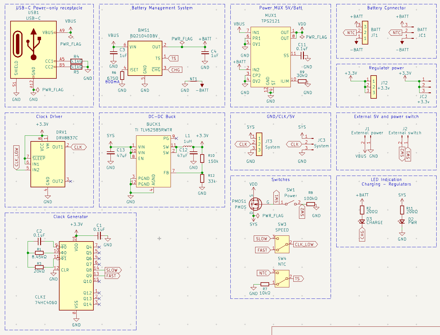
- USB-C receptacle
- Has 5.1k pull-down resistors for C-to-C power.
- This feeds VBUS, which in turn feeds the BMS directly, as well as the Power MUX
- BMS
- The BMS takes in power from USB and is configured to limit charge to 800mA into the battery.
- It outputs charge power to the +BATT power rail.
- It has a sink pin for powering an LED for CHARGE indication.
- Power MUX
- Takes in power from both VBUS (USB-C) and +BATT (Battery) and passes through whichever voltage is higher to the voltage regulator (VDD).
- Will take VBUS as priority, so when USB is plugged in, the battery is not being drawn from and will charge at maximum current.
- Voltage regulator (DC-DC buck)
- The voltage regulator will take power from the MUX and buck it down to a solid 3.3V with 3-3.5A current limit.
- Because it is not a buck/boost, if the battery ever gets to ≤3.3V, it will cut out.
- Clock generator and driver
- The clock and driver takes in 3.3V, and generates a clock signal based on the two resistors (R1 and R3) and a capacitor (C2)
- The generated clock signal has multiple speeds, over multiple pins. We use two pins with a solderable jumper to allow the user to change the clock frequency for faster or slower blinks.
- That clock signal is passed to a motor driver chip, which can handle push/pull for clock LEDs.
- Switches
- One physical switch - which actuates a PMOS - will disconnect and connect power from the MUX to the rest of the board. The BMS chip gets power directly from VBUS and remains unaffected.
- Clock speed "switch" is really just a solderable jumper pad, as there was no room to source an actual switch for this footprint.
- NTC "switch" is there to tell the BMS if there is a temperature sensor present. If your battery has a third wire for NTC temp sensing, you will solder this jumper to Y. If it does not, you will solder it to N, which pulls it down through a 10kΩ resistor.
- Connectors
- Castellated pads, solderable pins, and WAGO terminal blocks are broken out for a variety of mounting and wiring options.
- Castellated pads on the left and right side of the board are for external 5V power and external on/off switching. This was added so that a designer creating a display board could put their own USB port or power switch in a more convenient location without having to do anything more than drop the footprint (and throw a couple 5.1kΩ pulldown resistors for USB-C)
How did you design the board?
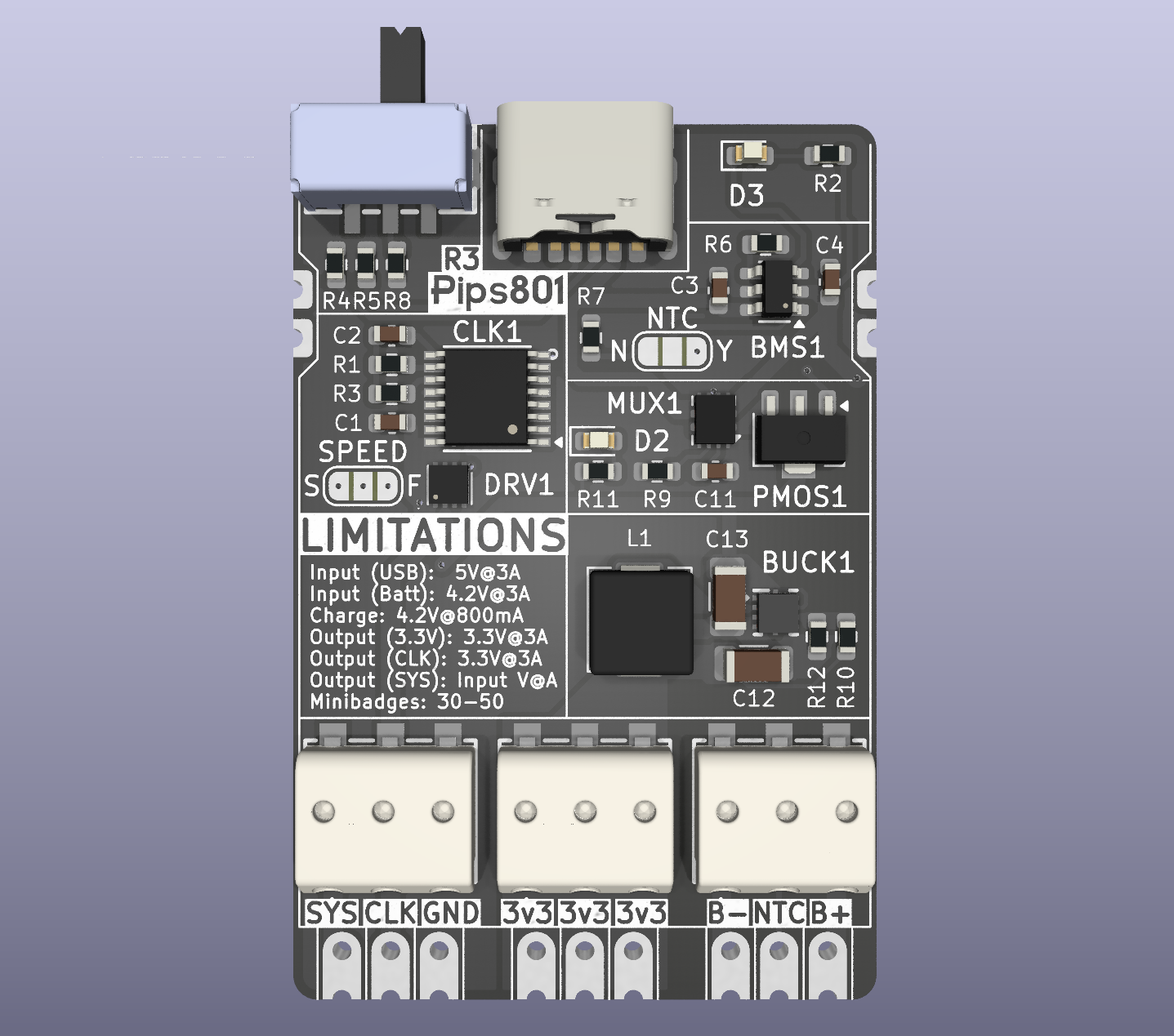
Below are some 3D renders of the board
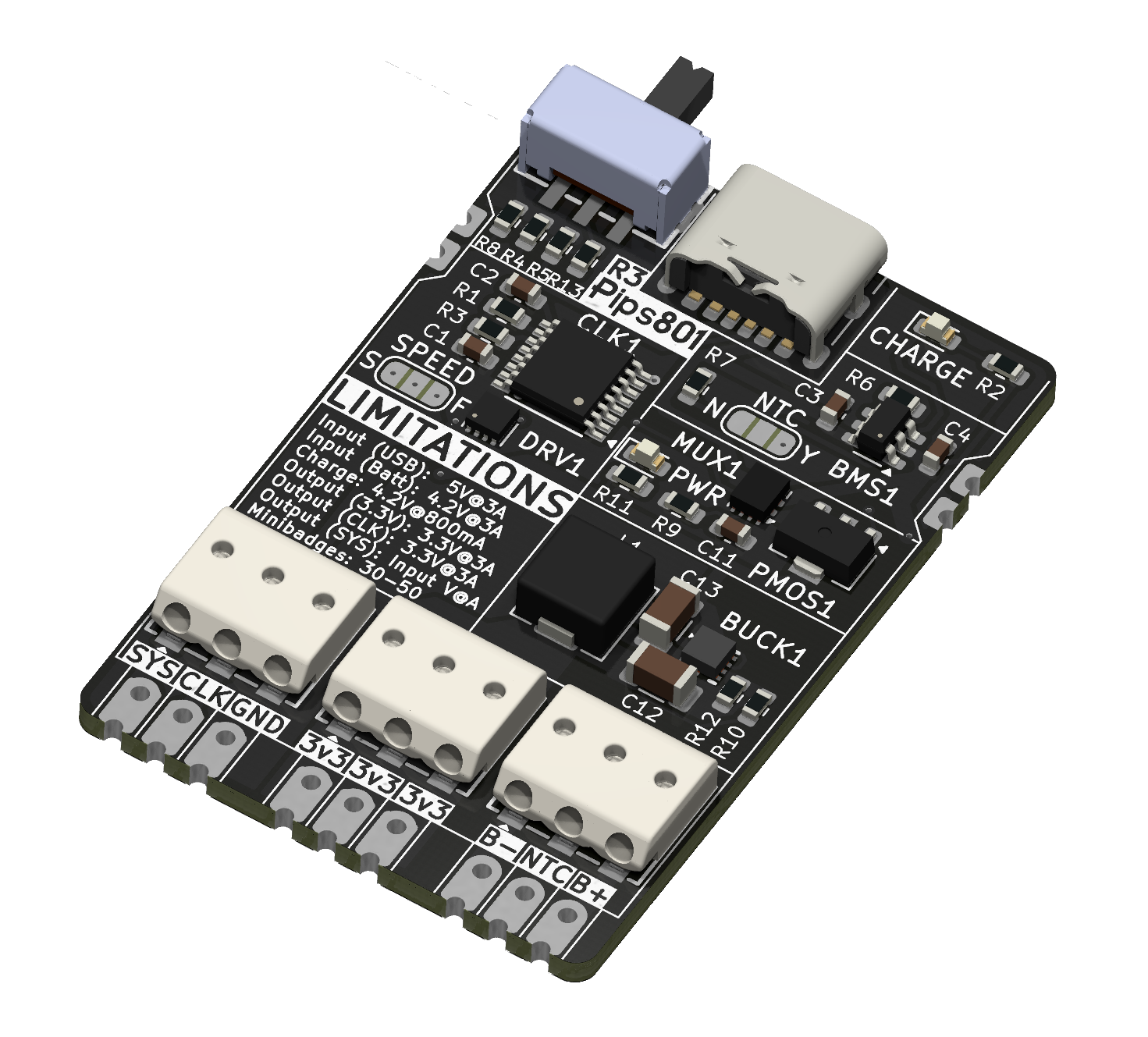
3D renders of the board (R3)
How did you iterate and revise the design over time?
The initial design used 3x 1A LDO regulators, which generate more heat and required three separate 3.3V rails to be implemented. This added an extra design challenge for display makers, as they had to create three different wiring pathways and split up all minibadges on the display evenly. These LDOs also generated a lot of heat during full load.
I eventually moved this over to to a single 3A buck regulator. It generates less heat, is much more efficient, and has a much smaller footprint. I believe it ended up being cheaper in the long run as well.
How did you manufacture the board?
I use JLCPCB for PCB and PCBA.
Wrapping up the project
Where is your source files?
You can find all of the source files (schematic, PCB, graphics, components, etc) on my GitHub!

How do I get one?
You can purchase one from my Tindie store!
Minibadge Display Devboard
A small PCB that allows you to create your own Minibadge displays!
What would you iterate on further?
I think with the third revision I have iterated as much as I can. I have solved all of the problems present with the design.
Any more "improvement", like more power or USB-C PD, would be broken out into a separate project with a new layout and different design goals.
Wrapping up this post
What did you learn from this?
Honestly, a lot.
- This was a great intro to more serious power-path management and what it takes to provide lots of amps at lower voltages. I feel more confident working on even higher-power requirement devices, such as PD voltages.
- First implementation of a switching regulator with an inductor. Can I just rant for a second and say that inductor footprints not being standardized is a huge pain in the ass.
- Normally for passive components, you select a footprint that works, and you just throw a component on there. Like LEDs, capacitors, resistors, and diodes.
- For inductors, you have to find the inductor you want to use first and copy its footprint. Nearly all inductors use a different custom footprint, and there are seriously no real standard sizes or footprints.
- Castellated pads are an expensive add-on for board manufacturing.
- This is my first time working with a BMS or a battery for a project. I chose a fairly weak and feature-less BMS, but it was perfect for the needs of this project.
What would you do different/better next time?
- Find a way around using castellated pads. While they help reduce vertical height for a board-to-board mount, they increase costs quite a bit and it makes prototyping hard. As far as for the finished product, it adds about $1 onto the BOM per unit.
- Implement USB-C Power delivery to be able to go beyond 15W. ≥35W is needed to power 100 minibadges (like a 10x10). This would require using a Voltage higher than 5V, and with that comes the need for both a 3.3V regulator and a 5V regulator.
- Use an even beefier voltage regulator with a wide range voltage input for PD. being able to provide 5-10A of 3.3V would be ideal.
How do you feel about this project?
I feel great! I learned some great skills, have taken them to newer projects yet to be published, and I think I made a niche product that is compelling enough to purchase.
I am excited to iterate on this idea and build a device that can power 100 or more minibadges and use USB-C power delivery.
I managed cost, DFM, and the BOM as best as I could, and touched on new areas to add to my skillset.